Around 1979, the degree of integration of semiconductor integrated circuits reached the 10-Kgate class, and high-performance minicomputers began to be widely adopted. This was also true within the Nippon Telegraph and Telephone Public Corporation (currently NTT), where the DIPS-11/5 Series was adopted more widely, and demand for small DIPS processors became evident in Japan.
Against this background of rising levels of integration and increasing demand for these logic elements, a DIPS-VLSI research plan was formulated in 1979, with the aim of establishing technology for achieving fully customized logic VLSI and technology based on such VLSI for achieving small DIPS processors. Work was started to make the technologies practical. The goals for VLSI technology were as follows: (1) element technology: CMOS 2 mM, (2) degree of integration: 20 Kgate/chip, (3) number of pins: 200 pins/chip, and (4) number of wiring layers: 3 layers.
At the time, one problem was what to select as the VLSI technology. From the standpoint of logic element performance, the common view at the time was that NMOS was superior. However, the highest priority was placed on ease of design for devices such as central processing units (CPUs) whose main constituent element was large-scale random logic. Thus, CMOS logic elements were used.
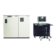
In the fall of 1981, a plan was formulated to develop a basic model of a small DIPS processor (the DIPS-V20). The goals of this plan included expanding application of DIPS to small-scale areas and developing applications to network internal communications processing; work was begun to make the technologies practical. The main points of the plan were a dual multiprocessor configuration, approximately 1/3 the performance of the DIPS-11 Model 5, 8-MB memory capacity, connection of small low-cost peripheral devices, and communications capability based on the data flow communications control (DFC) system.
From the standpoint of system composition, the aim was to use the DIPS architecture and achieve greater compactness for a general-purpose computer, while making the best use of software assets. Therefore, the system used a distributed function system where dedicated processors were provided for each of the three basic functions of the computer system (processing, storage, and communication) and then connected via a high-speed bus. In addition, development of the main logic elements was conducted by dividing the elements into three areas corresponding to the CPU, peripheral control (IOP), and communication control (ICA). The prototype was completed in March 1982.
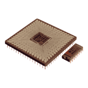
The core parts of the CPU, ICA, and IOP were achieved with 15 _ 20 Kgate fully customized VLSI based on CMOS 2 _ 2.5 megarules, and 5 _ 10 Kgate class master slice LSI was used for areas other than core parts. The system was on the cutting-edge of technology; it used 256-kbit/chip LSI memory for the main memory and achieved a maximum 16-MB main memory capacity. By actively using this VLSI, the system achieved a dramatic reduction in size and improvement in economy (DIPS Logic VLSI Chip Specifications).
The communication control processing part (ICA) was created by combining the multiple independent types of basic processing that accompany state transitions attributable to the occurrence of events and featured high processing parallelism and asynchronicity. Taking note of this point, the system used the DFC system. The DFC was a new communications control processing system developed independently by NTT's Electrical Communication Laboratories, who were working to achieve greater parallelism in processing by adopting the data flow machine concept. This system resulted in an improvement of about 2.5 times in the price/performance ratio compared to conventional systems.
| Item | CPU | IOP | ICA |
|---|---|---|---|
| Function | Arithmetic execution control | I/O control | Communications control |
| (Arithmetic bus width) | (32 bit) | (16 bit) | (8 bit x4) |
| Technology | CMOS | ||
| Number of transistors | 78 K | 67 K | 62 K |
| Chip size | 12 mm | 10 mm | 9.4 mm |
| Number of wiring layers | 3 layers (polysilicon 1 layer, metal 2 layers) | ||
| Power consumption | 750 mW Max. | ||
| Power supply voltage | 5 V single | ||


