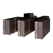
A series of supercomputers from Fujitsu. The vector processor FACOM VP-100 and FACOM VP-200 were announced as the company's first supercomputers in July 1982. These were developed, by exploiting the technology of the FACOM 230-75 APU, with the aim of achieving even higher performance, ease-of-use and affinity with the FACOM M Series of general-purpose computers. The series had the following features:
- (1)The VP architecture was defined based on analysis of actual FORTRAN programs
- Stress was placed on speeding up not only simple arithmetic operations, but also data sorting and conditional operations.
- (2)Vector instructions were executed in a high-speed operation pipeline, and a maximum performance of 500 MFLOPS was achieved with the VP-200
- (After announcement, this was enhanced to 571 MFLOPS)
- (3)Higher speed was achieved using high-speed semiconductor technology and high-density mounting
- -Employed state-of-the-art semiconductor technology -- ECL LSI with a gate delay time of 350ps and 400 and 1300 gates per chip, and high-speed RAM with an access time of 5.5ns
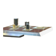
-Newly developed printed circuit board MCC (Multi-Chip Carrier) enabling high-density mounting of 121 LSI including RAM
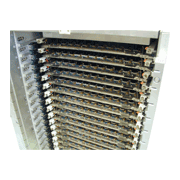
-Shortened wiring between LSI using a 50cm cubic stack structure - (4)Led the world in achieving a high data transfer capability by using static RAM (64 kilobit SRAM with access time of 55ns) for the main memory unit.
In January 1984, the #1 machine of the FACOM VP-100 Series (FACOM VP-100) began operating at the Nagoya University Plasma Research Center.
Later, the high-end FACOM VP-400, with improved performance, was added, and a processing performance exceeding 1GFLOPS was measured for the first time in the world. Also, the market was expanded by adding lower-end models: the FACOM VP-50 and FACOM VP-30. The FACOM VP Series E Models, enhanced versions of the FACOM VP-100 Series, were announced in July 1987.
| VP-30 | VP-50 | VP-100 | VP-200 | VP-400 | |||
|---|---|---|---|---|---|---|---|
| Announcement date | September 1986 | April 1985 | July 1982 | April 1985 | |||
| Maximum vector performance (MFLOPS) Figures in parentheses indicate enhancements after the initial announcement |
110 | 142 | 250 (→ 266→ 285) |
500 (→ 533→ 571) |
1142 | ||
| Vector process- ing unit |
Number of instru- ctions |
Scalar instructions | 195 | ||||
| Vector instructions | 83 | ||||||
| Registers | General- purpose registers |
16 (32bit) | |||||
| Floating point registers |
8 (64 bit) | ||||||
| Vector registers | 32KB | 64KB | 128KB | ||||
| Mask registers |
512B | 1KB | 2KB | ||||
| Buffer storage capacity |
32KB | 64KB | |||||
| Main device | 400, 1300 gates/chip, delay time 350ps/gate ECL LSI Access time 5.5ns 4Kbit/module RAM |
||||||
| Main memory unit | Memory device | Access time 55ns 64Kbit static RAM | |||||
| Capacity | 32/64 /128 MB |
64/128 /256 MB |
|||||
| Interleave count | 64/128 /128 way |
128/256 /256 way |
|||||
| Maximum number of channels | 32 | ||||||
(Note) The above specifications are from the time of announcement, and may have been changed due to later improvement.


