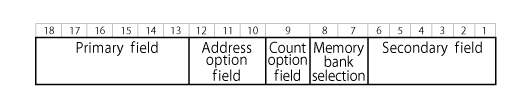
- Primary field:
- The primary command, such as load, store, add. These basic commands were executed in four or six clock cycles.
- Address option field:
- Register containing the address for memory reads and writes. Bits 10 and 11 indicated the M, L, P, or D register, and Bit 12 indicated either direct or indirect addressing.
- Count option field:
- This field specified the memory access or address change control (Count / Hold) or the word length for shift processing (Single / Double). The interpretation of this field was determined by the Address option field or the Primary field.
- Secondary field:
- Used as a secondary command, test conditions, parameters, or scratchpad memory addresses. The interpretation of this field was determined by the Address option field or the Primary field. Secondary commands were executed in the final clock cycle of the primary command.
A program created by combining LOGANDS was called a LOGRAM (which stood for “logical program”). Assembly language commands were implemented by LOGRAMs.
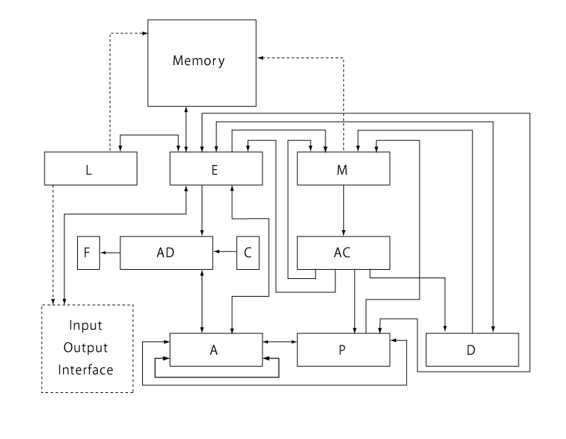
The main memory could hold 8K words, but this was expandable to 16K words or 32K words. One word consisted of 18 bits plus a parity bit. One word could contain three alphanumeric characters. The main memory was accessed from the operation circuitry, the I/O control unit (buffer controller), and the communications control unit (tele-control unit).
The operation circuitry and control circuitry were synchronous circuits timed to a 333 KHz clock pulse that was in sync with the memory cycle. The multiplication and division circuitry was also hardwired. The operations of up to three MELCOM 1530 processors could synced for direct data transfers by attaching a computer communications link (CCL) unit.
A buffer controller was included to perform I/O operations with peripheral devices. The buffer controller housed buffer memory, input channels, output channels, interrupt control circuitry, peripheral device control circuitry, and a power supply. With this controller, inputs, outputs, and calculations could be performed simultaneously. The buffer memory was a core memory with the same word length and access time as the main memory and could hold 384 characters. It had an 18-bit output register and a 132-bit output shift register, which were used for buffering outputs to slow devices such as card punches, line printers, paper-tape punches, and typewriters. Buffer memory was not used for input devices or high-speed output devices; an 80-bit input shift register buffered input data. These devices sent data to the main memory via interrupts or cycle-stealing, thereby increasing the system’s overall synchronous operation ratio.
A magnetic tape unit was used for large external storage. The magnetic tape units had seven tracks, which were IBM compatible, and a transfer speed of 41,700 characters per second. Up to eight units could be connected to the computer. Other devices that could be connected included a high-speed optical card reader with a scan speed of 1,650 cards per minute, a high-speed card reader/puncher with a punch speed of 300 cards per minute, a high-speed print-drum line printer with a print speed of 750 lines per minute with 132 characters per line, a 10-character-per-second typewriter, a paper-tape reader, and a paper-tape puncher. Also, up to four magnetic disks could be connected to the computer, each with a capacity of 228.3 x 106 bits (?32.5 million characters), an average access time of 190 milliseconds, and a maximum transfer speed of 697 x 103 bits per second.
The tele-control unit could handle up to 64 terminal stations, and each terminal station could be connected to up to 32 terminal devices.